
Introduction
Every NMR spectrometer requires a way to protect the sensitive receiver electronics from the high-power pulses used during excitation. This is the purpose of the Transmit/Receiver (TR) switch.
The classic switch for pulsed NMR instruments was introduced by Lowe and Tarr in 1968 and is still used in many home-built instruments up to today. Many labs have built their own version of the circuit but the basics have always stayed the same. The original circuit is shown in Figure 1.
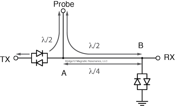
Figure 1: Passive T/R Switch after Lowe and Tarr.
In the figure above, TX is the connection to the transmitter, typically the output of the high-power pulse amplifier, and RX is the connection to receiver circuit. The circuit is entirely build from passive elements without the use of any active switches.
There two quintessential elements of the circuit are:
- The cross-diodes
- The λ/4 cable connected between points A and B (see figure 1)
A detailed description of the circuit is given in the original publication by Lowe and Tarr. A slightly more modern description is given in the review article written by David Hoult.
State of The Switch During Transmission
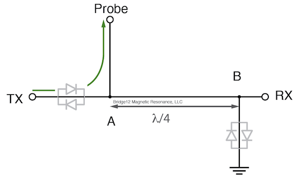
Figure 2: Circuit during a high-power RF pulse.
The principle of the switch relies on the non-linear behavior of a semi-conductor diode. At a forward voltage of below 0.7 V most diodes do not conduct and are of high impedance. However, once the forward voltage reaches a value of > 0.7 V the diode becomes low impedance and starts conducting current. It is this behavior that is used in the T/R switch to separate the transmit path from the receiver while sending high-power RF pulses.
In the T/R switch the diodes are arranges as pairs of anti-parallel cross-diodes. Pairs of anti-parallel diodes are used because the RF pulse is AC not DC. During a high-power RF pulse, both diode pairs have a low impedance and are conductive. The impedance transformation properties of the λ/4 cables ensures that a high impedance is in parallel with the transmitter and the probe. All power from the amplifier is sent to the probe.
State of The Switch After a Pulse
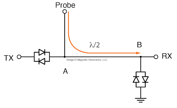
Figure 3: Circuit when no high-power pulse is applied.
When there are no high-power pulses the switch is in receiving mode. All diodes are high-impedance during this time and there is a direct electrical path from the probe to the pre-amplifier circuit.
Limitations of the Passive T/R Switch
The passive T/R switch after Lowe and Tarr is a robust design and has been used in many high- and low-frequency NMR instruments. It is a simple, and robust design that can easily be built in the lab. While it provides sufficient isolation between the TX and RX port during RF pulsing, the sensitivity is limited by two factors:
- The forward voltage of cross diodes. This leads to pulse shape distortions when using low-power RF pulses.
- The loss of the λ/4 cable. This is crucial for low-frequency operations, when λ/4 cables can become very long.
To overcome these limitations, active T/R switches based on PIN diodes are nowadays the standard in state-of-the-art instrumentation.
Despite these drawbacks it is an easy to understand design, greatly suited to teach fundamentals of the different aspects of the instrumentation used in NMR spectroscopy.
The Open-Source T/R Switch
By the time of writing this post the T/R switch by Lowe and Tarr et al. has been around for some 55+ years. Many labs have built their own versions and it’s performance can be tuned by carefully selecting which diodes to use in the circuit. Sometimes, these switches are built simply using a BNC (or N-type) tee, the corresponding cables and a two boxes with series cross-diodes and grounded cross-diodes.
Here we present a simple, PCB-based T/R switch board, based on a PCB, and off-the-shelf diodes and connectors. The T/R switch design is completely open source and published under the MIT open source license. All files including the CAD model, Gerber files (for PCB production), the Bill of Materials (BOM), and assembly instructions can be found at the OpenTRSwitch GitHub Repository.
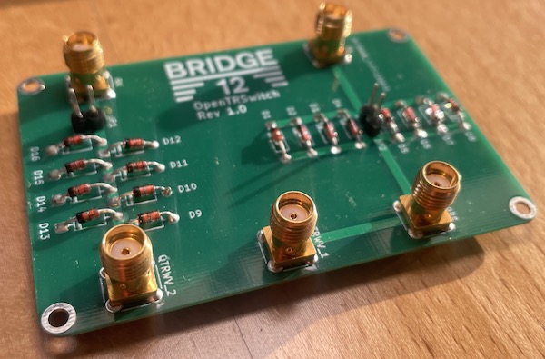
OpenTRSwitch
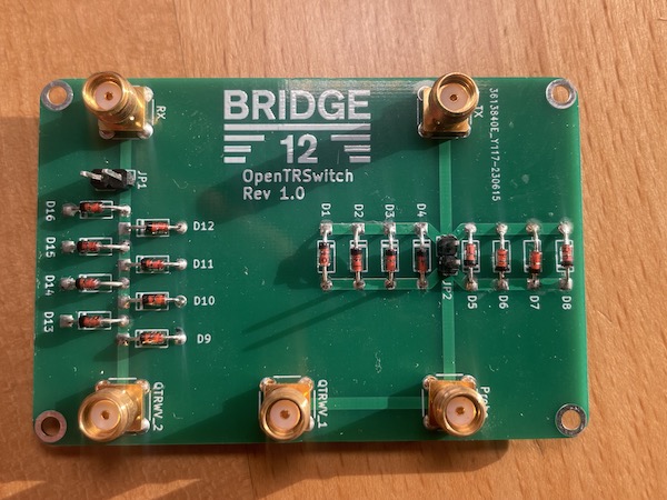
The OpenTRSwitch is a compact PCB. The current version has SMA connectors soldered directly to the board. A picture of the board is shown on the right. The board is simple to assemble and only requires standard off-the-shelf components.
Bill of Materials
The following table contains a list of all materials required to build the OpenTRSwitch. Some components for the λ/4 cable are only required to cut the cable to the correct length, such as the SMA tee, and the 50 Ohm termination.
| Component | Label | Qty. | Link |
|---|---|---|---|
| ———————– | ——————————— | ——— | ———– |
| OpenTRSwitch | |||
| OpenTRSwitch PCB | 1 | JLCPCB | |
| Diodes, model 1N4148 | D1 - D16 | 16 | DigiKey |
| SMA board connectors | RX, TX, Probe QTRW_1 QTRW_2 |
5 | DigiKey |
| 2-pin header | JP1, JP2 | 2 | DigiKey |
| Jumpers | 2 | DigiKey | |
| ———————– | ——————————— | ——— | ———– |
| λ/4-Cable | |||
| Crimp on SMA connectors | 2 | DigiKey | |
| RG-58 Cable | see below | DigiKey | |
| SMA tee (for testing) | 1 | DigiKey | |
| SMA 50 Ohm Termination | 1 | DigiKey |
In additon the following tools are required:
- Soldering iron, and solder.
- Crimping tool for SMA connector. These tools can become expensive. If you don’t have one ready, find the electronics shop of your physics department …
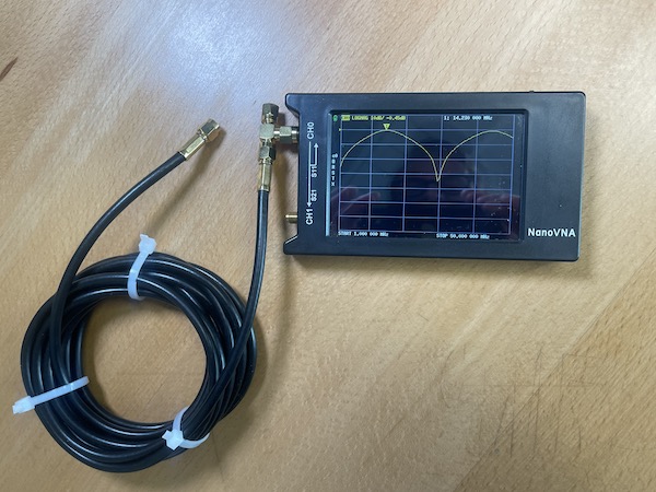
- Vector Network Analyzer (e.g. NanoVNA)
Note: A VNA is an extremely handy piece of equipment to have in the lab when working with RF circuits. They are used to measure reflection (S11) or transmission (S21) of an RF circuit. In recent years, many low cost device have become available. For example the NanoVNA is available for under 50 $ (including a calibration kit) and fulfills all requirements for this project.
Assembling the Board
The OpenTRSwitch is assembled in just a few simple steps:
- Start by soldering the cross diodes onto the PCB.
Pay attention to the direction of the diode, each diode pair will have an opposite direction. - Next, solder in the 2 pin headers. (These headers are only required if the board is tested on a VNA).
- In the final step, solder the SMA connectors to the board.
Making the Quarter-Lambda Cable
The λ/4 cable needs to have the correct length. At low frequencies the cable becomes quite long and it doesn’t have to be cut very high precision. The following table gives the length for a λ/4 cable to be used for proton and carbon NMR spectroscopy at 15 and 2.5 MHz, respectively:
| Nucleus | Frequency | Lenght (mm) | Length (in.) |
|---|---|---|---|
| 1H | 15 MHz | xxx mm | xxx in. |
| 13C | 2.5 MHz | xxx mm | xxx in. |
To calculate the length of the cable first convert the frequency of the experiment to the wavelength and multiply the result with the propagation constant for the cable. The propagation constant is given in the datasheet of the cable. For example, the propagation constant for RG-58 is 0.68.
There is a very simple but elegant way to make sure the λ/4 cable has the correct length. Attach a SMA tee to the (S11) port of the VNA. Terminate one leg of the SMA tee with a 50 Ω termination and connect λ/4 cable to the other leg of the tee, leaving the end of the cable unconnected.
Adjust the start frequency of the VNA to 1 MHz and the stop frequency to a large value, say 50 MHz.
If the λ/4 cable has the correct length, the (S11) value measured at this frequency will be at a maximum (here 14.23 MHz, see picture). If the VNA was calibrated the measured (S11) value corresponds to the insertion loss of the cable. In this case the insertion loss is 0.45 dB.
If the cable is too long, the maximum (S11) value will be at a lower frequency. If the cable is too short, the (S11) maximum will be shifted to a a higher frequency.
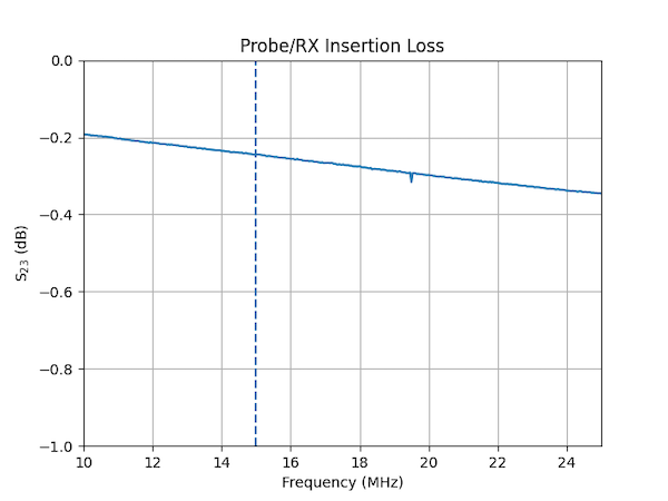
Measuring S21 (Probe/RX)
To measure the insertion loss from the probe to the output of the switch (RX) connect port 1 of the VNA to the SMA connector labeled Probe, and connect port 2 to the connector labeled RX. Do not install any of the jumpers. You should see a similar response as shown in the figure to the right.
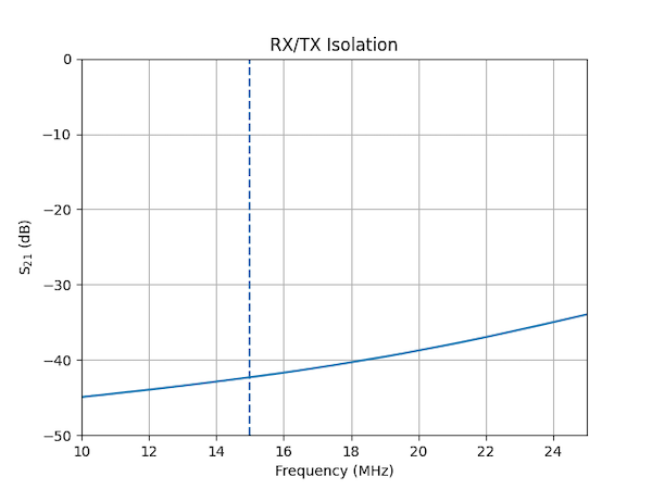
Measuring S21 (TX/RX)
To measure the isolation between TX and RX connect port 1 of the VNA to the SMA connector labeled TX, connect port 2 to the connector labeled RX, and install both jumpers. You should see a similar response as shown in the figure to the right.
That’s it. That’s everything you need to know to assemble the OpenTRSwitch and run some basic characterization. If the circuit behaves as described above it is ready to be used in the NMR spectrometer.
Bibliography
-
Lowe, I., and C. Tarr. “A Fast Recovery Probe and Receiver for Pulsed Nuclear Magnetic Resonance Spectroscopy.” Journal of Physics E: Scientific Instruments 1 (1968): 320–22. https://doi.org/10.1088/0022-3735/1/3/312.
-
Hoult, David I. “Receiver Design for MR.” In EMagRes, edited by Robin K. Harris and Roderick L. Wasylishen, 1–21. Chichester, UK: John Wiley & Sons, Ltd, 1996. https://doi.org/10.1002/9780470034590.emrstm1137.
Disclaimer
- This document describes the OpenTRSwitch an Open-Source Transmit/Receive Switch for NMR spectroscopy
- Assembling and using the OpenTRSwitch is entirely on your own risk. Bridge12 cannot be held responsible for any damage done to any equipment (e.g. test equipment or spectrometers) as a result of testing this device
- Please make sure to read these instructions carefully
This is teaching equipment. By no means should this low-cost TR switch be compared with a high-end front-end of a high-fidelity NMR spectrometer.